Presseinformation

Shaping the Future of Microchip Manufacturing: Erik Loopstra (ZEISS) and Vadim Banine (ASML) Receive European Inventor Award 2018 in Popular Prize Category (Only in EN)

Award-winning contributions to the development of extreme ultraviolet (EUV) lithography enable the next generation of microchips

8. Juni 2018 · 2 Min. Lesedauer

Oberkochen, Germany / Paris, France | 8 June 2018 | ZEISS Group

Yesterday in Paris, engineer Erik Loopstra (ZEISS) and physicist Vadim Banine (ASML) received the European Inventor Award 2018 in the Popular Prize category. The European Patent Office presents the prestigious award to those inventors selected by the public from among 15 finalists. Together with their engineering and research teams, Loopstra and Banine developed ground-breaking inventions for extreme ultraviolet (EUV) lithography.

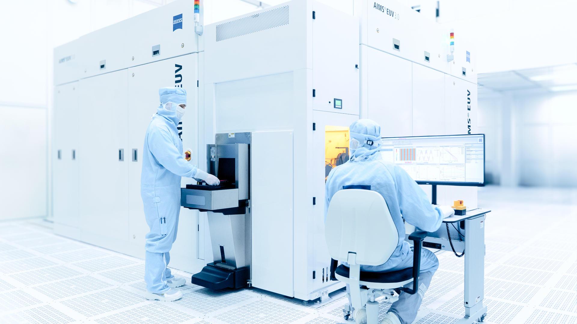
EUV lithography enables an unprecedented level of precision for creating geometric structures on wafers, which are the foundation for microchips.

EUV technology became market-ready in 2017. It is now possible to manufacture a new generation of chips more quickly and easily than with older production methods. The new technology not only saves chip fabs time and costs, but most importantly drives innovations in the areas of home electronics, healthcare, entertainment, self-driving cars, robotics and artificial intelligence.

First presented by the European Patent Office in 2006, the European Inventor Award is one of the most important innovation prizes in Europe. It honors individual inventors and teams of inventors whose innovations assist in the search for technical solutions to the greatest challenges of our time.

  • Blick auf Bühne beim European Inventor Award 2018

    Today in Paris, engineer Erik Loopstra (ZEISS) and physicist Vadim Banine (ASML) received the European Inventor Award 2018 in the Popular Prize category. The European Patent Office presents the prestigious award to those inventors selected by the public from among 15 finalists. Together with their engineering and research teams, Loopstra and Banine developed ground-breaking inventions for extreme ultraviolet (EUV) lithography.

Erik Loopstra named new ZEISS Fellow

In honor of his groundbreaking achievements, Erik Loopstra was recently named a ZEISS Fellow, the highest rung on the ZEISS Expert Ladder. The Executive Board of the ZEISS Group congratulated him on his appointment and thanked him for his excellent work to date.

Dr. Karl Lamprecht, Member of the Executive Board at ZEISS responsible for the Semiconductor Manufacturing Technology segment, drew particular attention to Loopstra's personal qualities: "He not only leads teams as an expert in his field, but also guides them and fosters a team mindset. His opinion carries a lot of weight among developers and leading experts. Erik Loopstra winning this year's European Inventor Award in the Popular Prize category demonstrates the importance of his expertise beyond the world of ZEISS and underscores his international reputation."

About ZEISS

ZEISS is an internationally leading technology enterprise operating in the fields of optics and optoelectronics. The ZEISS Group develops, produces and distributes measuring technology, microscopes, medical technology, eyeglass lenses, camera and cinema lenses, binoculars and semiconductor manufacturing equipment. With its solutions, the company constantly advances the world of optics and helps shape technological progress. ZEISS is divided up into the four segments Research & Quality Technology, Medical Technology, Vision Care/Consumer Products and Semiconductor Manufacturing Technology. The ZEISS Group is represented in more than 40 countries and has over 50 sales and service locations, more than 30 manufacturing sites and about 25 research and development centers around the globe.

In fiscal year 2016/17 the company generated revenue approximating €5.3 billion with around 27,000 employees. Founded in 1846 in Jena, the company is headquartered in Oberkochen, Germany. Carl Zeiss AG is the strategic management holding company that manages the ZEISS Group. The company is wholly owned by the Carl Zeiss Stiftung (Carl Zeiss Foundation).

Semiconductor Manufacturing Technology

With its broad product portfolio and expertise, the Semiconductor Manufacturing Technology segment of ZEISS covers a variety of key processes in the production of microchips. Its products include semiconductor manufacturing optics – notably lithography optics – as well as photomask systems and process control solutions for semiconductor manufacturing. Thanks to ZEISS technology, microchips are becoming increasingly more powerful, more energy-efficient and more affordable. The electronic applications of these ongoing enhancements enable global progress in many disciplines such as technology, electronics, communication, entertainment, mobility and energy.

Semiconductor Manufacturing Technology is headquartered in Oberkochen. Other sites include Jena, Rossdorf and Wetzlar in Germany, as well as Bar Lev (Israel) and Pleasanton, CA (USA). During fiscal year 2016/17, the segment generated revenue of €1.2 billion and employed around 2,900 people.

Press Photos

  • Der Europäische Erfinderpreis 2018 in der Kategorie "Popular Prize"

    Heute wurden der Ingenieur Erik Loopstra (ZEISS) und der Physiker Vadim Banine (ASML) in Paris mit dem Europäischen Erfinderpreis 2018 in der Kategorie Popular Prize ausgezeichnet. Das Europäische Patentamt vergibt die prestigeträchtige Auszeichnung an Erfinder, die von der Öffentlichkeit aus 15 Finalisten ausgewählt wurden. Gemeinsam mit ihren Ingenieur- und Forschungsteams haben Loopstra und Banine bahnbrechende Erfindungen für die EUV-Lithografie (Extreme Ultraviolet Lithography) entwickelt.

    Seiten: 1
    Dateigröße: 1 MB

Share this article